Imec has announced the launch of SPINS (Semiconductor Pilot line for Industrial Quantum NanoSystems), a strategic initiative designed to bridge the gap between academic research and industrial manufacturing for quantum processors. The €50 million project, co-funded by the European Union’s Chips Joint Undertaking (Chips JU) and participating member states, is one of six specialized pilot lines established under the EU Chips Act. The consortium includes 25 partners across Europe, including Fraunhofer IPMS, VTT, CEA-Leti, Infineon, and STMicroelectronics.
The SPINS project focuses on the development of semiconductor-based spin qubits, leveraging existing CMOS manufacturing expertise to scale toward fault-tolerant quantum systems. The initiative is currently prioritizing three technology platforms: Si/SiGe, Ge/GeSi, and SOI (Silicon-on-Insulator). By establishing a “lab-to-fab” pathway, SPINS intends to provide standardized Quantum Process Design Kits (PDKs) and Multi-Project Wafer (MPW) runs, allowing startups and SMEs to validate designs on industrial-grade 300mm infrastructure.
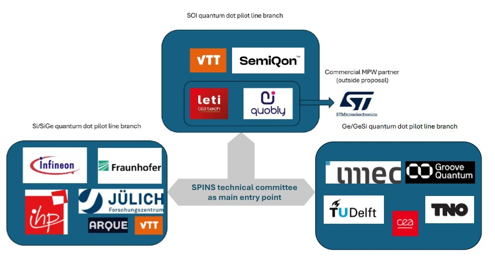
Technical Roles and Process Integration
The consortium distributes technical responsibilities across its Research and Technology Organizations (RTOs) to address specific bottlenecks in qubit fabrication:
- High-Resolution Patterning: Fraunhofer IPMS leads the high-resolution structuring of qubit elements. Using state-of-the-art cleanroom infrastructure in Dresden, the institute handles lithography steps beyond the capabilities of optical methods, ensuring the reproducible patterning required for Si/SiGe-based chips.
- Foundry-Compatible Processes: CEA-Leti leads the development of PDKs and the execution of MPW runs. In collaboration with Quobly and STMicroelectronics, it is working on foundry-compatible FD-SOI processes and the integration of superconducting layers into back-end-of-line (BEOL) processes.
- Heterostructure Development: Imec is exploring the Ge/GeSi platform on 300mm wafers, focusing on Heterogeneous integration and record-fidelity silicon quantum dot qubits. This work is complemented by IHP and Siltronic, who provide heterostructure substrates and fabrication support.
Cryogenic Control and Characterization
Scaling to millions of qubits requires precise control electronics that can operate at temperatures near absolute zero. VTT and SemiQon are leading the development of ultra-low-power cryo-CMOS technology to manage qubit drive voltages without exceeding the thermal limits of dilution refrigerators. Additionally, a high-volume characterization framework is being established by the University of Jyväskylä, Groove Quantum, and TNO to provide fast feedback on device performance at quantum-relevant temperatures (1-4K).
Strategic Alignment with the EU Chips Act
The SPINS pilot line is part of a multimodal European strategy to ensure technological sovereignty in quantum hardware. It operates alongside other pilot lines dedicated to:
- Photonics (P4Q): Coordinated by University of Twente (NL).
- Ion Traps (CHAMP-ION): Coordinated by SAL (AT).
- Superconducting Qubits (SUPREME): Coordinated by VTT (FI).
- Diamond (DIREQT): Coordinated by CNR (IT).
- Neutral Atoms (Q PLANET): Coordinated by Pasqal (FR).
By utilizing 300mm CMOS lines and industrial process readiness, the SPINS consortium aims to reduce the entry barriers for the European quantum ecosystem and establish a predictable path toward mass-producible, high-TRL (Technology Readiness Level) quantum chips by 2031.
For the official press release regarding the launch of SPINS, visit imec here. Detailed technical information on Fraunhofer IPMS’s lithography and 300mm cleanroom contributions is available here and here.
April 18, 2026
