Researchers from the IMDEA Software Institute, Nokia Bell Labs, the Complutense University of Madrid, Aalto University, and Quobly have developed an FPGA-based hardware architecture for the real-time decoding of quantum LDPC codes. Published on ArXiv, the design manages correlated error arrays within a structural layout optimized for latency, physical area, and power consumption. The architecture utilizes targeted resource reuse loops rather than unrestricted hardware parallelization to process complex multi-qubit syndromic dependencies, addressing classical computational processing bottlenecks that challenge the physical scaling of the quantum error correction (QEC) layer.
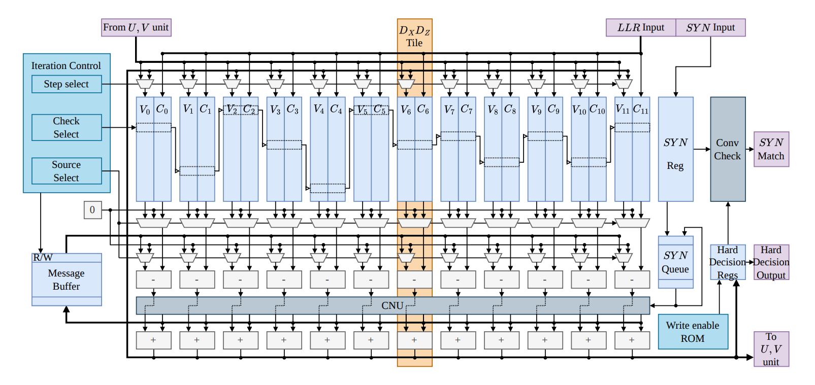
The internal layout of the decoder maps straight to the specialized Graph Augmentation and Rewiring for Inference (GARI) framework. Standard decoding routines typically process spatial X and Z error coordinates independently, which reduces tracking fidelity when phase and bit-flip parameters become linked through combined Y-type faults. The GARI transform alters the underlying detector error model matrix by separating the correlated variables and eliminating short 4-cycles involving Y errors, substituting the entangled graphs with structured U and V coordinate dependencies. This algebraic reconfiguration allows the hardware to distribute joint decoding tasks over decoupled execution paths, suppressing harmful message correlations while maintaining iterative information exchanges between the error domains.
[ Complex Correlated Graph ] ──► [ GARI Transform Matrix ] ──► [ DX, DZ Serial BP Unit ] ──► [ Memory Real-Time Update ]
                                                               [  U,  V Parallel Unit  ] ──► [ Crossbar Interconnect  ]
To execute this restructured matrix, the architecture splits processing tasks between a belief propagation (BP) core and a parallelized tracking block. The primary DX and DZ matrices are routed through a memory-based, serially scheduled BP unit that updates calculation parameters sequentially according to normalized Min-Sum rules. Concurrently, the independent check structures of the U and V matrices are parallelized within separate hardware tiles to synchronize processing intervals with the serial core. Data transfers between these alternating computing passes are handled by a modular Crossbar interconnect that operates as an N-to-N pipeline router using binary radix sorting stages, bypassing explicit classical controller logic to prevent routing congestion and data-bus stall conditions.
The hardware implementation was evaluated on an AMD VCU19P FPGA (and mapped to VU29P FPGA fabrics) to decode the [[144,12,12]] bivariate bicycle code over a window of 12 consecutive syndrome measurement rounds. To minimize internal routing pressure and memory footprint, the architecture applies numerical quantization constraints, restricting input Log-Likelihood Ratios (LLRs) to 6 bits, check-node messages to 8 bits, and variable-node values to 10 bits while approximating the numerical precision of classical floating-point tracking models. Running at an operating frequency of approximately 274 MHz through AXI-Stream ports, the pipelined execution loop delivers an average decoding latency of 596 ns per round, satisfying real-time decoding constraints under hardware-realistic correlated noise distributions.
By reducing individual processing requirements, the design allows multiple independent decoding cores to be integrated onto a single piece of silicon. The individual core consumes a restricted footprint consisting of 7.5% of total logic Look-Up Tables (LUTs), 3.5% of registers, and 26% of internal Block RAM (BRAM) elements, which can be partially mapped onto URAM blocks to lower memory pressure. This resource efficiency enables a three-decoder ensemble configuration to run simultaneously inside a single VCU19P FPGA board. This spatial density lowers the device overhead needed to run multi-core decoders, allowing a complete tracking ensemble of 24 concurrent decoders to deploy across eight physical hardware devices instead of the 48 boards required by fully parallelized alternative architectures.
The detailed silicon resource allocations, matrix transformation derivations, and routing latency benchmarks can be reviewed in the full pre-print manuscript available on arXiv here.
June 24, 2026
