Moving to standard CMOS wafer manufacturing is very helpful for certain modalities but not all. The real competitive advantages come from fabrication throughput—measured in wafers per hour (WPH)—and cycle time (i.e. the time from design submission to tested device). This is where manufacturing economics meets quantum roadmaps.
The IonQ-SkyWater Acquisition: A Case Study in Vertical Integration
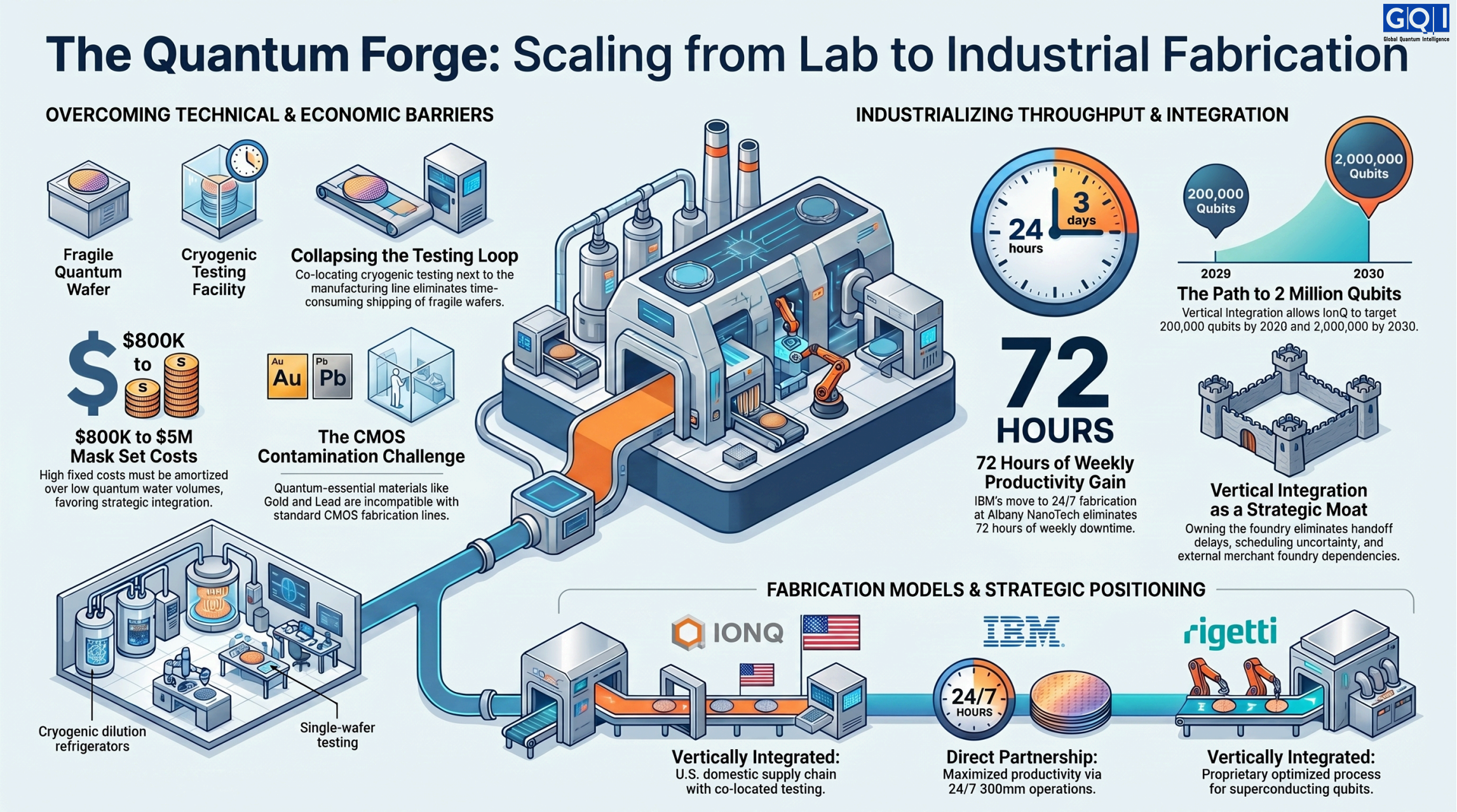
In January 2026, IonQ announced its intent to acquire SkyWater Technology, one of the largest U.S.-based pure-play semiconductor foundries, for approximately $1.8 billion. The transaction, which received shareholder approval in May 2026 and is expected to close in the second or third quarter of 2026, represents a clear signal that manufacturing is now an important consideration when developing quantum hardware.
Why vertical integration matters for cycle time:
With embedded access to its own trusted foundry, IonQ gains direct control over design, wafer fabrication, packaging, and testing under one roof. This eliminates the handoff delays and scheduling uncertainty of merchant foundry engagement.
The roadmap acceleration:
IonQ now expects to begin functional testing of 200,000-qubit machines (enabling over 8,000 ultra-high-fidelity logical qubits) in 2029. The company’s roadmap targets a 2,000,000-qubit machine by 2030.
Supply chain positioning (manufacturing to chip):
The combination creates a U.S.-based manufacturing supply chain from design through fabrication and packaging, likely focused on photonic integrated circuits (PICs) and trap development. This aligns with government procurement frameworks for secure domestic quantum hardware.
What this signals for the industry:
Fault-tolerant quantum roadmaps increasingly depend on manufacturing methodology and quality control. Metrics, like line roughness, take on new, critical dimensions, as they have a direct impact on qubit coherence. Competitors still relying on shared research fabs or merchant foundries face longer cycles and less control over these specialized process parameters.
Fabrication Throughput: The 24/7 Advantage
Not all fabrication facilities operate at the same speed. The difference in operating hours translates directly into faster design cycles.
IBM’s Albany advantage:
IBM’s quantum chips are fabricated at NY CREATES’ Albany NanoTech Complex (and soon Anderon), which processes wafers 24/7. Previously, IBM’s quantum chips were fabricated at their Yorktown Heights 200mm research-scale lab, which ran 16 hours a day, 5 or 6 days a week, resulting in ~ 72 hours of lost productivity per week. The issue is not only the advanced 300mm technology itself; it is that high-productivity fabs are the only facilities where this level of 24/7 operation makes economic sense. IBM is targeting that maximized productivity. As a further step, IBM is team with the U.S. Department of Commerce to create a new company called Anderon that will focus exclusively on quantum fabrication.
Christy Tyberg, IBM Distinguished Engineer of Quantum Fab Technology & Infrastructure, stated: “If we had not started processing our chips at Albany using 300mm technology, we wouldn’t have achieved the success required to pull off our development roadmap”.
The Testing Bottleneck
For quantum technology, a significant hurdle to rapid iteration is often the testing phase for the chips. To measure whether the core qubits work as intended, the devices must be cooled to near absolute zero (a few milliKelvin in most cases). Because the cooling process is difficult to do on a massive scale, it often becomes the primary bottleneck that delays getting new chips from the lab to the market.
The co-location solution:
SkyWater Technology is addressing this delay at its Minnesota facility by housing these cryogenic testing stations right next to the manufacturing line. By testing the chips under the same roof where they are built, the company eliminates the time lost shipping fragile wafers to outside labs.
This builds on important industry breakthroughs, like a collaboration between Intel, Bluefors, and Afore, which resulted in the first machine capable of testing entire wafers of chips at 1.6 Kelvin before they are even cut apart. To accommodate other types of quantum technology, SkyWater is also building in-house testing beds for light-based (photonic) chips, further speeding up the development cycle.
Quantum-Specific Constraints: Materials and Testing
Gold incompatibility with CMOS:
During GQI’s interview with Dr. Gilbert at Skywater, he highlighted that although gold is completely incompatible with standard CMOS processes, it is needed for some quantum packaging applications. Gold contaminates CMOS fabrication lines and cannot be easily removed. This forces quantum companies to choose between dedicated tooling or packaging in separate facilities for the crucial gold depositing.
Microsoft’s recently announced Majorana 2 chip led to a breakthrough in stability. The key improvement stems from the material switch from aluminum to lead. However, lead is traditionally banned from standard chip-making facilities. The chemical baths and highly purified water used to wash standard chips can easily strip the lead away, spreading contamination throughout the factory’s fluid systems. Manufacturing chips like the Majorana 2 at scale requires highly specialized precautions to ensure millions of dollars of factory equipment aren’t ruined by these incompatible materials.
The Economic Tension: Volume vs. Fixed Costs
Producing quantum chips on standard semiconductor lines presents a fundamental economic tension. The fixed costs of a mask set ($800K–$5M+) and EDA tool licenses ($200K–$1M+ annually) must be amortized over the number of wafers produced.
For high-volume commercial chips producing thousands of wafers per year, these fixed costs are negligible per die. For quantum chips, where annual wafer volumes may be in the dozens or hundreds, the per-die fixed cost is orders of magnitude higher.
This is why the IonQ-SkyWater vertical integration model is strategically significant. It allows IonQ to:
- Avoid huge CAPEX: SkyWater already owns the fabrication tools. IonQ does not need to buy them.
- Dedicate pilot lines: SkyWater can allocate specific equipment to quantum processes without contaminating mainstream CMOS production.
- Iterate without merchant foundry scheduling uncertainty: IonQ controls its own queue priority.
The economic tension is not that quantum cannot be fabricated on standard lines. It is that the fixed costs must be justified by strategic value, not unit volume.
From Lab to Fab: The Design Automation Gap
Scaling to thousands or millions of qubits requires electronic design automation (EDA) tools adapted for quantum. Most quantum companies already use GDSII format and some form of design rule checking. The gap is in design rules specific for quantum product manufacturing.
USTC’s wafer-scale Q-EDA stack:
Researchers at the University of Science and Technology of China (USTC) have demonstrated a complete pipeline converting GDSII files into manufacturing-ready instructions. Key achievements include:
- 504 qubits fabricated on a single chip
- 76 geometric design rule checks, of which nine are quantum-specific to address unique challenges in superconducting circuit fabrication (e.g. minimum coplanar waveguide gap of 3μm to control two-level system losses, Josephson junction overlap tolerances of ±50nm for critical current control)
- 300mm CMOS production lines achieving transmon coherence times exceeding 100μs, marking a transition from proof-of-concept to engineered systems
The USTC paper is available on ArXiv. However, it is important to qualify that these tolerances (±50nm) are not exceptionally precise by CMOS standards—line roughness in advanced nodes is measured in nanometers. The challenge is not meeting the tolerances but ensuring the right metrics (coherence, two-level system density) are prioritized.
A process methodology like this—with quantum-specific design rules embedded in standard EDA flows—is a significant enabler for migration to standardized CMOS fabrication.
The Competitive Landscape: Foundry Access Can Be a Moat
Current quantum hardware supply chain positioning varies significantly by company:
| Company | Fab Access Model | Wafer Size | Strategic Positioning |
| IonQ (via SkyWater) | Vertically integrated (acquisition) | 200mm | DMEA Category 1A Trusted Foundry, U.S. domestic supply chain, co-located testing |
| IBM | Direct partnership (Albany NanoTech plus soon Anderon) | 300mm | 24/7 operation, 75% more productive capacity than 16/5 |
| Rigetti | Vertically integrated | 150mm | Provides optimized process for their own proprietary superconducting qubit process |
| OQC | Merchant foundry | 200mm | Cost-effective at current scale |
| Others (Diraq, spin qubits) | Partner fabs | 300mm | Access to advanced nodes but less control |
Strategic observation: The quantum hardware industry is fragmenting into those who control their fabrication supply chain and those who do not. Vertical integration (IonQ) and exclusive partnerships (IBM with Albany NanoTech), and standalone foundries (Anderon) create moats. Merchant foundry dependency introduces uncertainty in pricing, scheduling, and access to advanced nodes.
Testing plays a critical role here. Companies with co-located testing (SkyWater Minnesota) or integrated test capabilities (IBM/Anderon with in-line wafer testing) can close the iteration loop faster than those shipping wafers to external test facilities. This directly reduces cycle time and X-factor.
The supply chain is increasingly defined by extreme supplier concentration in several critical categories—dilution refrigeration, helium-3, quantum-grade lasers, isotopically enriched silicon-28, and cryo-CMOS controllers. These constraints affect all modalities but compound for companies without direct fab access.
The Path Forward
To maintain competitiveness in quantum hardware, companies must be able to:
- Achieve high fabrication throughput (WPH) through 24/7 fab access or dedicated pilot lines
- Minimize cycle time through co-located testing and short design-to-measurement loops
- Control specialized process parameters (line roughness, material purity) that affect qubit coherence
- Access advanced tools without bearing the full CAPEX of ownership
- Integrate testing into the fabrication workflow to collapse iteration time
Companies that master these manufacturing disciplines will have an advantage in the next phase of the industry.
This is the second in a series examining quantum hardware manufacturing. For deeper analysis of fabrication trends, supply chain dynamics, and modality-specific roadmaps, GQI subscribers can access our full manufacturing database and custom briefing services. To learn more, contact GQI at info@global-qi.com or reach out directly to clay@global-qi.com.
June 23, 2026
