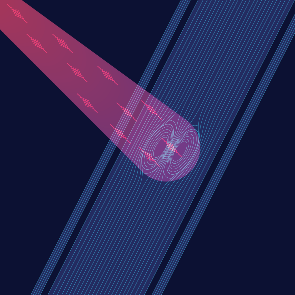
Physicists at the National Institute of Standards and Technology (NIST) have developed a magnetic shielding architecture that scales the physical width of superconducting nanowire single-photon detectors (SNSPDs) up to 0.1 mm (100 µm)—100 times wider than standard nanoscale SNSPDs and 20 times wider than previous state-of-the-art implementations. Published in Optica, the design uses active current “rails” to eliminate edge-current crowding, suppressing dark-count noise rates by 10 orders of magnitude while achieving near-unity detection efficiency across the mid-infrared spectrum.
| [ Wide-SNSPD Structural Architecture & Performance Metrics ] | ||
|---|---|---|
| Physical Specifications | Noise & Sensitivity Metrics | Industrial & Scalability Impact |
| • 100 µm (0.1 mm) Active Wire Width | • 10¹⁰ Drop in Dark Count Rate | • Standard Microfabrication Compatibility |
| • Adjacent Nb Magnetic “Rails” | • Near-Unity Efficiency at 4 µm (Mid-IR) | • Elimination of E-Beam Lithography Yield Limits |
| • Overcomes Magnetic Pearl Barrier | • Extended 1550 nm Detection Plateau | • Polarization-Insensitive Photonic Coupling |
Technical Breakthrough: Neutralizing the Pearl Limit
SNSPDs represent a critical hardware component for photonic quantum computing (e.g., active feed-forward routing in measurement-based architectures), quantum key distribution (QKD), and deep-space optical communications. However, conventional detectors have been historically constrained to nanoscale widths (~100 nm) due to edge current crowding:
- Current Density Redistribution: In wide superconducting strips, the Meissner effect forces current density to concentrate heavily along physical edges. This current pileup lowers the energy threshold for magnetic vortices to breach the wire, triggering false voltage pulses (dark counts) well below the material’s theoretical critical current (Idep).
- Active Magnetic Cancellation: The NIST architecture places current-biased niobium (Nb) rails parallel to a central tungsten-silicide (WSi) strip. The magnetic self-field generated by these rails directly opposes and cancels the perpendicular self-field at the edges of the detector. This pushes peak current density inward, eliminating the edge-vortex entry mechanism and allowing operation at the material’s intrinsic performance limit.
- Mid-Infrared Quantum Sensing: Operating near Idep drastically reduces the minimum photon energy needed to trigger a hotspot across the wire width. On 20 µm wide devices, the architecture demonstrated near-unity internal detection efficiency (IDE) at 4 µm wavelengths, extending high-efficiency single-photon counting far into the mid-IR band.
Strategic Analysis: Commercial & Manufacturing Implications
Transitioning SNSPD footprints from nanoscale to micrometer-scale dimensions directly alters the economic and operational trajectory of photonic hardware:
- Elimination of Nanofabrication Bottlenecks: Standard nanoscale SNSPDs require complex, low-throughput electron-beam (e-beam) lithography, limiting wafer yields and manufacturing scalability. Micrometer-scale wide-SNSPDs can be patterned using conventional, high-throughput optical photolithography.
- Simplified Optical Coupling & High-Count Arrays: Photonic integrated circuits (PICs) and free-space quantum communications currently suffer high insertion losses when alignment drifts relative to a 100 nm target. A 100 µm active detection footprint vastly improves alignment tolerances, lowers packaging costs, and enables dense 2D detector arrays for multiphoton state processing.
- Polarization Agnosticism: Nanoscale meander geometries are inherently sensitive to photon polarization angles. The wide-strip geometry eliminates this directional dependency, allowing unpolarized or scattered light (such as quantum signals transmitted through turbulent atmospheric channels or biological tissue) to be registered with uniform probability.
This development directly addresses the yield, cost, and optical coupling constraints currently impeding the industrial deployment of large-scale photonic quantum processors and regional QKD networks.
Review the official announcement via NIST News here, and access the peer-reviewed research paper on Optica here.
August 25, 2026