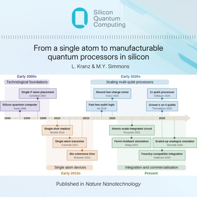
In a Comment published in Nature Nanotechnology, Silicon Quantum Computing (SQC) Head of Quantum Engineering Ludwik Kranz and CEO Michelle Simmons trace the 25-year evolution of phosphorus-in-silicon quantum processors (the 14/15 platform) from single-atom transistor demonstrations to commercial atomic-scale products.
The perspective outlines the technological progression of atomic-precision fabrication, where scanning tunneling microscope (STM) hydrogen lithography has transitioned from a manual research tool into an automated industrial process capable of placing phosphorus atoms with 0.13-nanometer spatial accuracy at rates exceeding hundreds of thousands of qubit registers per day. By leveraging high-purity, isotopically purified silicon (28Si) and epitaxial encapsulation, the platform achieves single-qubit gate fidelities exceeding 99.99% and coherence times beyond 30 seconds.
| [ Historical Evolution of the Silicon 14/15 Quantum Platform ] | ||
|---|---|---|
| Development Era | Key Technological Milestones | Architectural & Commercial Significance |
| • Foundations (1998–2000s) | • Kane proposal for phosphorus nuclear spins in silicon • STM single-atom placement lithography | • Established atomic precision fabrication using hydrogen resists and phosphine precursors. |
| • Single-Atom Devices (2010s) | • Single-shot electron spin readout • Single-atom transistor fabrication • 30-second nuclear spin coherence times | • Demonstrated functional sub-nanometer nano-electronic devices and defect-free spin encapsulation. |
| • Multi-Qubit Scaling (2020s) | • Record-low 1/f charge noise in epitaxial devices • Fast two-qubit exchange logic • 11-qubit multi-register quantum processor | • Achieved two-qubit gate fidelities above 99.9% and executed multi-qubit algorithms above fault-tolerance thresholds. |
| • Industrial Integration (Present) | • 15,000 quantum dot analog simulators • Fermi-Hubbard 2D atom array simulations • Automated 0.13 nm STM hydrogen lithography | • Deployed commercial analog simulators and quantum feature generators into classical HPC and AI pipelines without full QEC requirements. |
The authors note that the remaining path to universal fault tolerance centers on industrial-scale 3D integration with foundry-built classical control electronics and cryogenic interconnects. Because electron wavefunctions in silicon extend across only a few nanometers, the platform operates with higher thermal headroom than superconducting circuits, allowing utility-scale processors with hundreds of thousands of physical qubits to operate within a single dilution refrigerator.
Review the full Comment article in Nature Nanotechnology here and access additional details on the Silicon Quantum Computing Portal here.
October 14, 2026