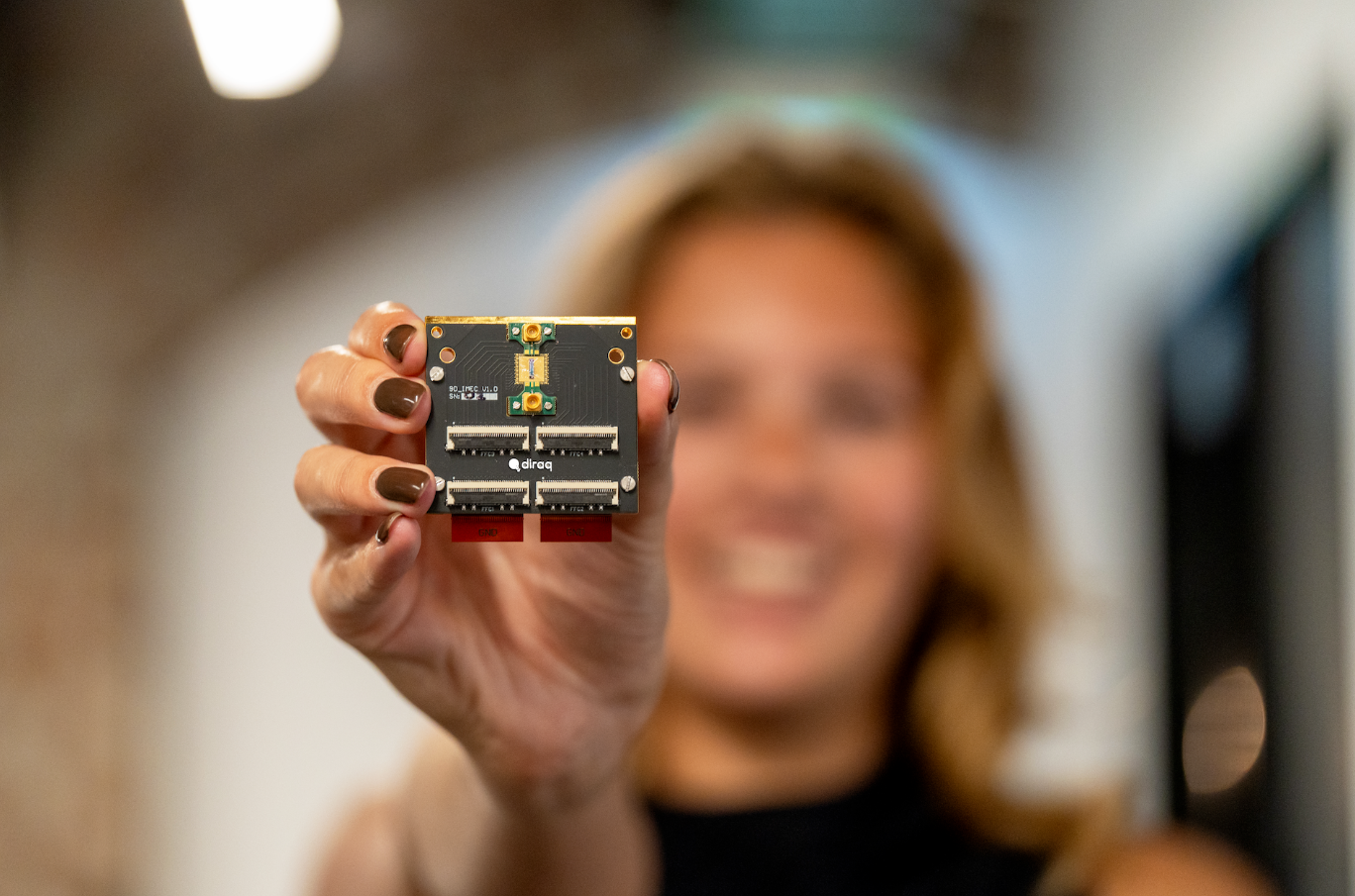
Silicon quantum computing developer Diraq has officially opened its U.S. Technology Hub in Santa Monica, California. Launching with a 20-person engineering team, the new facility targets integrated circuit (IC) design, cryogenic CMOS architecture, device modeling, and machine learning. Diraq plans to double the hub’s headcount over the next 12 months to support the trans-Pacific scaling of its CMOS-compatible silicon spin-qubit processors.
| [ Diraq Trans-Pacific Engineering Infrastructure Stack ] | ||
|---|---|---|
| U.S. Operations Nodes | Core Engineering & Testing Scope | Sydney Headquarters & R&D |
| • Palo Alto (U.S. HQ & Ecosystem) | • Cryo-CMOS & IC Design (LA Hub) | • Sydney Centre of Excellence |
| • Santa Monica (Engineering Hub) | • Device Modeling & ML Architecture | • Device Fabrication & Physics R&D |
| • Chicago (Measurement Lab) | • Cryogenic Qubit Testing & Verification | • Target 2029 Product Launch |
Tri-Node U.S. Footprint and Trans-Pacific Integration
The Santa Monica facility marks Diraq’s second major U.S. infrastructure expansion within a single month—following the launch of its dedicated measurement and cryogenic testing laboratory in Chicago. Together with its corporate base in Palo Alto, the three-node U.S. network complements the company’s primary R&D headquarters and manufacturing partner ecosystem in Sydney, Australia:
- Palo Alto, CA (Commercial Headquarters): Serves as the primary node for corporate operations, semiconductor foundry partnerships, and Silicon Valley ecosystem integration.
- Santa Monica, CA (Engineering Hub): Focuses on multi-disciplinary engineering, including IC architecture, software stacks, cryo-CMOS control electronics, and automated device calibration algorithms.
- Chicago, IL (Quantum Laboratory): Houses dedicated dilution refrigeration and measurement infrastructure for high-throughput qubit testing, cryo-CMOS characterization, and hardware verification.
Leveraging Commercial CMOS Foundries for Million-Qubit Density
Unlike architectures requiring bespoke materials processing, Diraq fabricates silicon spin qubits using standard commercial complementary metal-oxide-semiconductor (CMOS) foundry processes. This approach is designed to leverage existing semiconductor manufacturing infrastructure to integrate qubit arrays and control electronics onto a single silicon die:
- Cryo-CMOS Integration: Bringing qubit drive, readout, and multiplexing circuits directly onto the silicon substrate reduces the interconnect bottleneck and thermal load associated with routing thousands of coaxial cables into a dilution refrigerator.
- Scale and Product Roadmap: By expanding its trans-Pacific design capability between Australia and the U.S., Diraq aims to transition from individual device demonstrations toward fault-tolerant systems, targeting its first commercial product launch by 2029.
Led by Founder and CEO Andrew Dzurak, the expansion positions Diraq to draw from Southern California’s concentration of semiconductor, defense, and aerospace engineering talent.
Review the official announcement via Diraq here, and examine our previous coverage of Diraq Opens a U.S. Office in Palo Alto, California here, Diraq Establishes First U.S. Quantum Laboratory at Chicago’s IQMP On-Ramp Hub here, and Diraq’s Quantum Leap: New Commercial Lab Opens in Sydney here.
August 25, 2026