
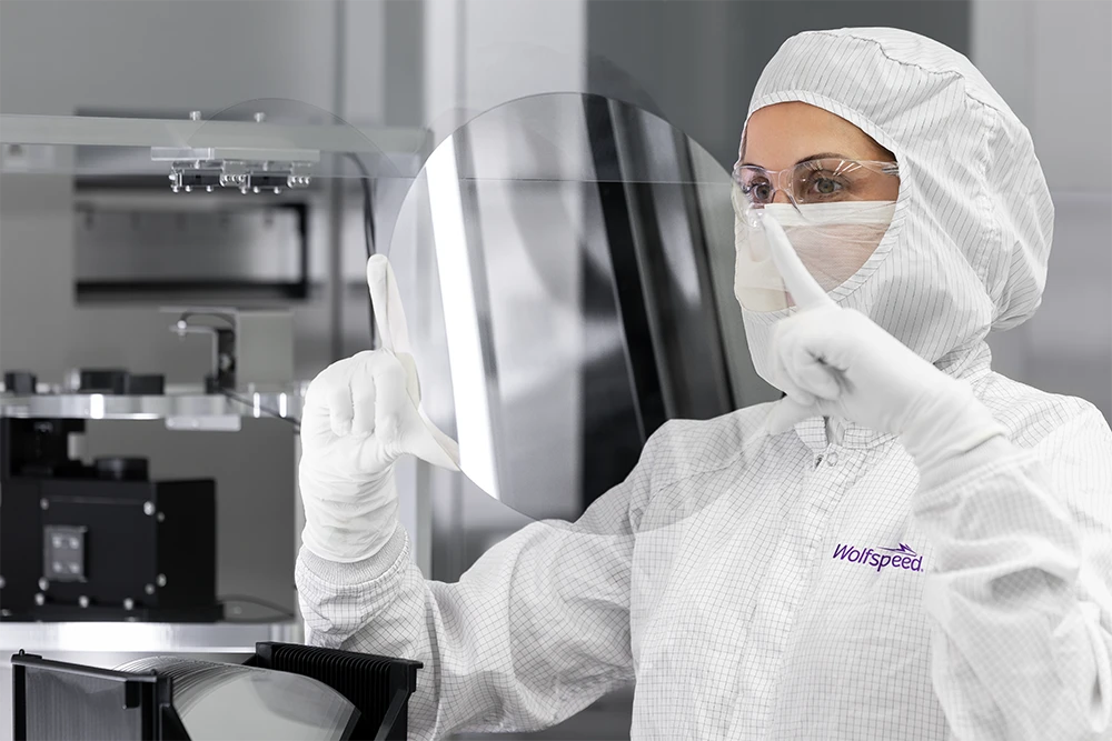
Semiconductor substrate manufacturer Wolfspeed, Inc. (NYSE: WOLF) has announced the commercial launch of its proprietary optical-grade transparent silicon carbide (TSiC™) wafer technology. While initially targeted at augmented reality (AR) near-eye display waveguides, the single-crystal 4H-SiC material is being introduced across the quantum hardware supply chain as a scalable wafer platform for solid-state spin qubits, low-loss integrated quantum photonics, and cryogenic packaging substrates. The commercial availability of 150 mm and 200 mm substrates—with 300 mm wafers currently sampling—marks an inflection point for quantum photonic integration, addressing the wafer-scale fabrication bottlenecks that historically constrained wide-bandgap quantum devices.
The TSiC™ technology builds on Wolfspeed’s high-purity semi-insulating (HPSI) crystal growth and chemical mechanical polishing (CMP) processes, utilizing patented defect-reduction techniques to achieve an optical absorption coefficient ≤ 0.05 cm−1 across visible wavelengths (450 nm to 650 nm). In quantum computing and quantum networking, single-crystal 4H-SiC acts as a host matrix for optically addressable spin defects, including neutral divacancies (VSi-VC) and silicon vacancies (VSi), which exhibit long spin coherence times and emit near the telecom O- and C-bands. Combined with a high refractive index (~2.65), low optical birefringence, and high thermal conductivity (up to 4.9 W/cm·K at room temperature), the material enables monolithic integration where spin qubits, optical waveguides, and single-photon routing channels are fabricated within the same crystal layer.
| Wolfspeed Optical-Grade TSiC™ Substrate Specifications | ||
|---|---|---|
| Product Parameter | Technical Specification | Quantum Hardware & Photonic Relevance |
| Crystalline Polytype | Single-crystal 4H-SiC (On-axis orientation) | Preserves crystallographic symmetry required for stable color-center dipole alignment and low acoustic loss. |
| Commercial Diameters | 150 mm, 200 mm (300 mm sampling) | Enables high-volume CMOS cleanroom processing, overcoming diamond’s millimeter-scale wafer ceiling. |
| Optical Absorption (450–650 nm) | ≤ 0.05 cm−1 | Minimizes photon attenuation and thermal dissipation in integrated optical waveguides and resonant cavities. |
| Total Thickness Variation (TTV) | ≤ 1.5 μm (3 mm edge exclusion) | Ensures sub-micron film uniformity during wafer bonding and thin-film SiC-on-insulator (SiCOI) smart-cut processing. |
| Surface Roughness (Sq) | ≤ 1 nm (Double-sided CMP polish) | Suppresses interfacial scattering loss in evanescently coupled photonic circuits and optical resonators. |
| Wafer Geometry (Bow / Warp) | +10 μm / < 20 μm | Mitigates mechanical strain and structural dephasing in lithographically patterned cryogenic devices. |
The commercial rollout of optical-grade silicon carbide directly challenges synthetic diamond as the primary host material for solid-state color-center quantum hardware. While diamond nitrogen-vacancy (NV) centers possess mature quantum sensing protocols and long room-temperature coherence, diamond remains limited to small-area substrate “mosaics” that cannot scale within commercial 200 mm or 300 mm semiconductor semiconductor manufacturing lines. In contrast, Wolfspeed’s ability to supply optical-grade substrates at 200 mm (Part No. W4WPH0S-N-0200) allows quantum developers to leverage standard deep-ultraviolet (DUV) lithography and plasma etching tools to produce thousands of entangled spin-photon nodes on a single wafer.
However, translating bulk substrate availability into fault-tolerant quantum processors introduces device-level hurdles. Realizing low-loss SiCOI photonic circuits requires perfecting smart-cut thin-film transfer onto oxidized silicon wafers without inducing lattice damage that quenches spin-defect emission. Furthermore, maintaining optical coherence at cryogenic temperatures demands precise control over isotopic purity (depleting nuclear spin-carrying 29Si and 13C isotopes) to suppress spectral diffusion and nuclear-spin bath dephasing in color-center registers.
Substrate configurations and sample evaluation requests are available via Wolfspeed’s Optical-Grade Materials Catalog here, with corporate background provided in the official Wolfspeed Investor Announcement here.
In GQI Portal
The players behind the news
The team that writes QCR tracks every company, deal and technology in the GQI Factory, GQI's verified database of the quantum industry. Next up: every story linked to its players, coming to QCR's paid plans.
- Players Companies and institutions across the quantum industry, by segment.
- Scorecards How the players compare on hardware, software, funding and more.
Newsletter
QCR Alerts in your inbox
The latest reporting and analysis from Quantum Computing Report. Free, unsubscribe any time.