Quantum hardware developer EeroQ has published peer-reviewed experimental results demonstrating the selective, two-dimensional transport of electrons on superfluid helium using a commercial silicon control architecture. Published in Physical Review Applied (“Selective shuttling of electrons on helium using a CMOS control platform“), the research validates the structural integrity of the company’s mobile spin-qubit transport layer. By moving electron packets across an atomically smooth liquid helium film condensed over a standard microelectronics chip, the system achieves lossless, long-distance charge transport—bypassing the material impurities and charge traps that typically cause phase decoherence and signal degradation in solid-state quantum architectures.
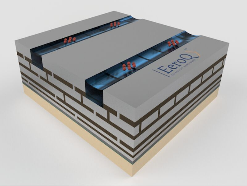
                         [ EeroQ Wonder Lake Hardware Stack ]
  Substrate Layer     ──► Superfluid liquid helium film condensed onto a solid-state CMOS chip.
  Fabrication Node    ──► SkyWater Technology 130-nm commercial silicon foundry process.
  Control Multiplexing──► 14 external control lines driving 128 independently addressable channels.
  Transport Metric    ──► Zero detectable charge loss over 10^9 repetitive shuttling cycles (kilometers in aggregate).
The Architecture of Superfluid Charge-Coupled Devices
The primary engineering constraint when scaling trapped-electron or quantum-dot platforms is the wiring bottleneck. As qubit counts increase, conventional architectures typically require a dedicated, non-local control line for every single trapping site, leading to massive heat routing and geometric congestion over the dilution refrigerator stack. EeroQ addresses this scaling barrier by organizing its “Wonder Lake” prototype chip as a macro-scale Charge-Coupled Device (CCD), a multiplexing layout similar to the silicon sensor grids used in digital imaging hardware.
The underlying micro-architecture consists of a two-dimensional network of microchannels filled with a thin layer of liquid helium. Because liquid helium is clean of the random chemical dangling bonds and lattice defects found in solid semiconductors, it forms a perfectly uniform potential surface for floating electrons. Using just 14 global control lines, the on-chip CMOS circuitry selectively guides electron packets containing tens of particles down to isolated, single-electron qubits through any of 128 parallel transport pathways. This “unit cell” layout is repeated 32 times across the monolithic array, creating high-density connection corridors between localized storage areas, on-chip electrostatic sensors, and prospective gate zones.
Lossless Kilometric Transport and All-to-All Scaling
Supervised by a joint engineering panel including lead author K.E. Castoria and CEO Nick Farina, the hardware was fabricated at U.S. commercial semiconductor foundry SkyWater Technology using a standard 130-nm CMOS process flow. During validation testing, the team subjected the electron packets to continuous, high-frequency clocking sequences:
- Endurance Threshold: The electron packets successfully completed at least 109 continuous transfer cycles without a single verifiable charge dropping from the potential wells.
- Spatial Displacement: In aggregate, the electron arrays collectively traveled tens of kilometers across the microchannel layout while remaining securely floating above the substrate.
- Connectivity Geometry: The routing efficiency enables all-to-all qubit connectivity across the physical layout, permitting distant qubits to be mechanically shuttled next to each other for fast, two-qubit entangling gates.
This capability to dynamically shuffle information across a standard microelectronics footprint simplifies the layout requirements for high-distance topological error correction, allowing EeroQ to leverage existing commercial semiconductor manufacturing lines to scale its hardware without building bespoke cleanroom fabrication tools.
Review the official corporate announcement on the EeroQ Newsroom here, and audit the peer-reviewed publication directly through Physical Review Applied here.
July 10, 2026