

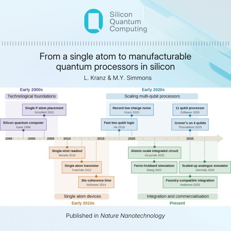
In a Comment published in Nature Nanotechnology, Silicon Quantum Computing (SQC) Head of Quantum Engineering Ludwik Kranz and CEO Michelle Simmons trace the 25-year evolution of phosphorus-in-silicon quantum processors (the 14/15 platform) from single-atom transistor demonstrations to commercial atomic-scale products.
The perspective outlines the technological progression of atomic-precision fabrication, where scanning tunneling microscope (STM) hydrogen lithography has transitioned from a manual research tool into an automated industrial process capable of placing phosphorus atoms with 0.13-nanometer spatial accuracy at rates exceeding hundreds of thousands of qubit registers per day. By leveraging high-purity, isotopically purified silicon (28Si) and epitaxial encapsulation, the platform achieves single-qubit gate fidelities exceeding 99.99% and coherence times beyond 30 seconds.
| [ Historical Evolution of the Silicon 14/15 Quantum Platform ] | ||
|---|---|---|
| Development Era | Key Technological Milestones | Architectural & Commercial Significance |
| • Foundations (1998–2000s) | • Kane proposal for phosphorus nuclear spins in silicon • STM single-atom placement lithography | • Established atomic precision fabrication using hydrogen resists and phosphine precursors. |
| • Single-Atom Devices (2010s) | • Single-shot electron spin readout • Single-atom transistor fabrication • 30-second nuclear spin coherence times | • Demonstrated functional sub-nanometer nano-electronic devices and defect-free spin encapsulation. |
| • Multi-Qubit Scaling (2020s) | • Record-low 1/f charge noise in epitaxial devices • Fast two-qubit exchange logic • 11-qubit multi-register quantum processor | • Achieved two-qubit gate fidelities above 99.9% and executed multi-qubit algorithms above fault-tolerance thresholds. |
| • Industrial Integration (Present) | • 15,000 quantum dot analog simulators • Fermi-Hubbard 2D atom array simulations • Automated 0.13 nm STM hydrogen lithography | • Deployed commercial analog simulators and quantum feature generators into classical HPC and AI pipelines without full QEC requirements. |
The authors note that the remaining path to universal fault tolerance centers on industrial-scale 3D integration with foundry-built classical control electronics and cryogenic interconnects. Because electron wavefunctions in silicon extend across only a few nanometers, the platform operates with higher thermal headroom than superconducting circuits, allowing utility-scale processors with hundreds of thousands of physical qubits to operate within a single dilution refrigerator.
Review the full Comment article in Nature Nanotechnology here and access additional details on the Silicon Quantum Computing Portal here.
In GQI Portal
The players behind the news
The team that writes QCR tracks every company, deal and technology in the GQI Factory, GQI's verified database of the quantum industry. Next up: every story linked to its players, coming to QCR's paid plans.
- Players Companies and institutions across the quantum industry, by segment.
- Scorecards How the players compare on hardware, software, funding and more.
Newsletter
QCR Alerts in your inbox
The latest reporting and analysis from Quantum Computing Report. Free, unsubscribe any time.