Introduction
After almost 20 years of development, Microsoft has developed a controllable topological qubit module design that they intend on scaling up very quickly to produce a 1 million qubit error corrected quantum computer within a few years. In theory, a topological qubit could provide the optimal type of qubit because it combines three desirable properties together without requiring tradeoffs: Reliability, Speed, and Size. In practice, the topological qubit has been very difficult to build because it depends on leveraging Majorana zero modes (MZMs) which hitherto was only a theoretical particle and does not occur naturally in nature. A key advantage of the topological approach is that information is stored in a non-local manner so it should be much harder for noise to upset the state. Saying this another way, some error protection is built into the hardware architecture making it easier to create error correction codes that together with the hardware provide greater protection against errors.
Device Construction
After years of research, Microsoft’s development team has been able to develop a recipe for creating these Majoranas using a heterostructure that includes aluminum, an intermediate layer, and an Indium-Arsenide based semiconductor. These materials are very carefully deposited onto the layers using a molecular beam epitaxy process on an atom-by-atom basis to create a new form of matter which they call a topoconductor.
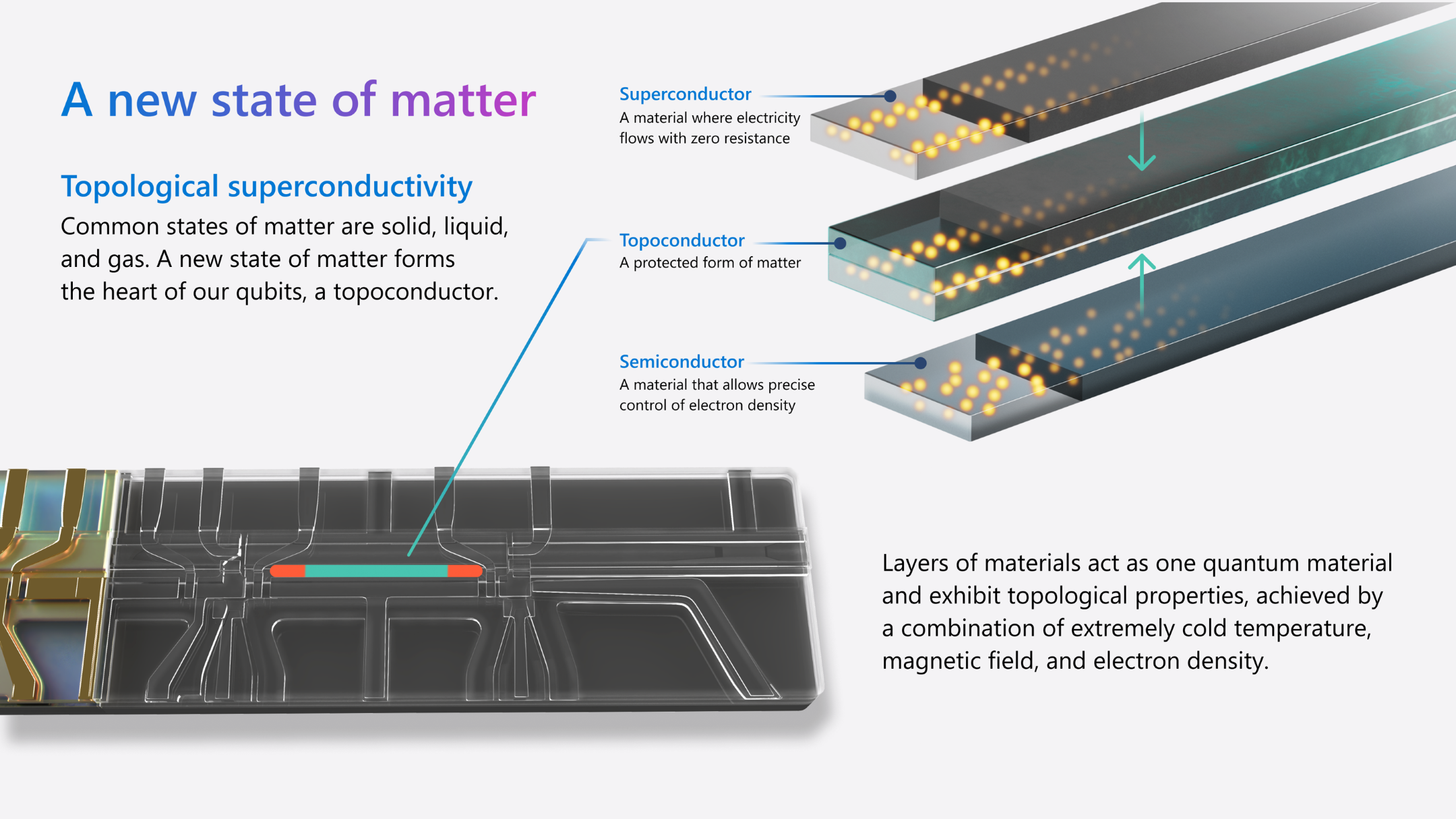
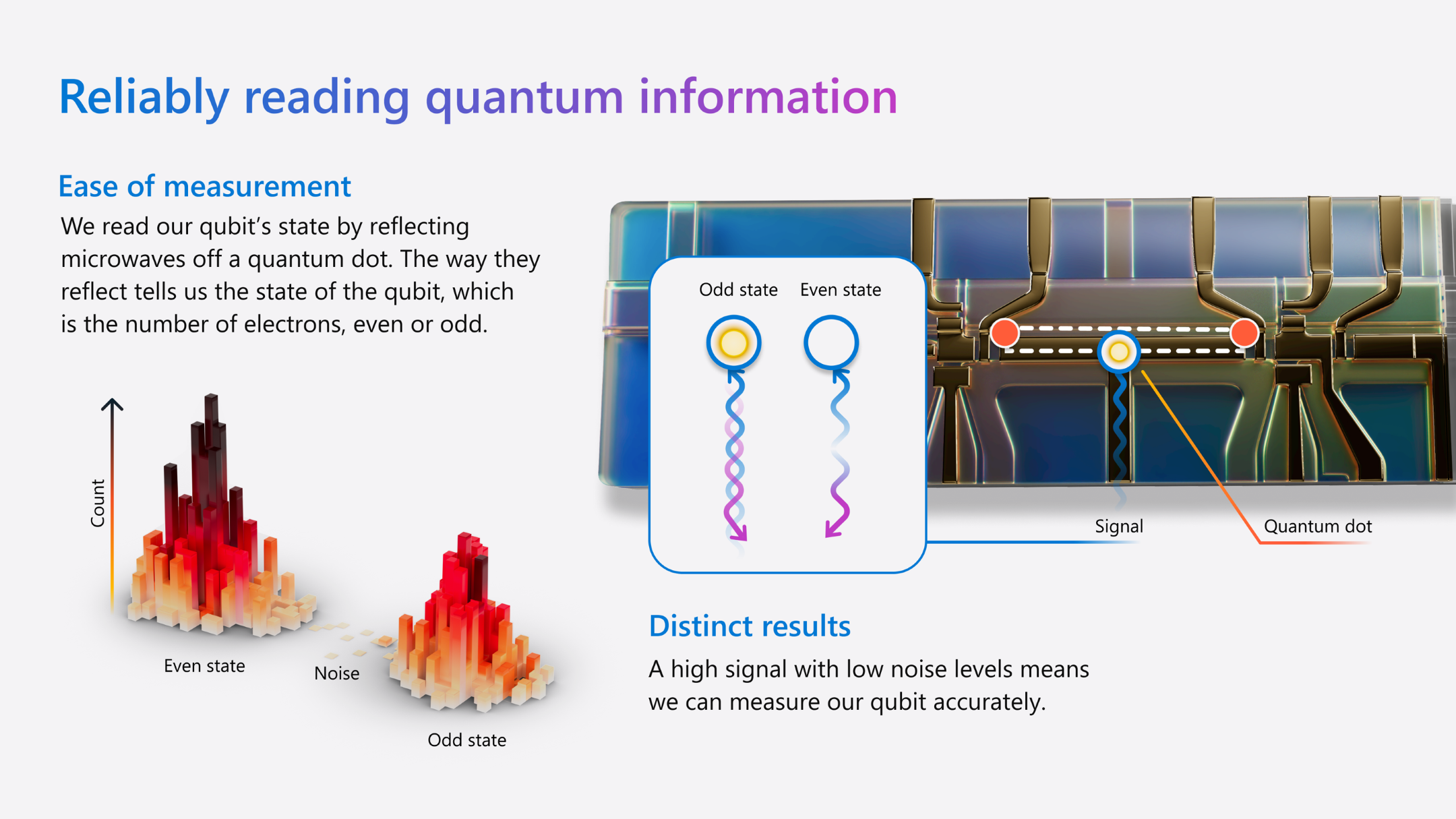
This topoconductor is kept under very low temperatures and a magnetic field and the state can read out using a long and thin quantum dot as shown in the diagram below. In a normal superconductor the electrons always form what are called Cooper pairs. But the Majorana’s are different because the device could be in a state where there is one unpaired electron left over. The circuitry in the Microsoft design can sense the difference between an even and odd number of electronics by reflecting microwave signals off the quantum dot and measuring a capacitance change via a phase shift in the reflected signal. Microsoft claims their readout approach is so sensitive it can tell the difference between 1,000,000,000 and 1,000,000,001 electrons, e.g. Even or Odd.
To form a single qubit two of these topoconductors are used together along with an aluminum wire in the middle to form an “H on its side” pattern as shown in the leftmost layout in Figure 4. The qubit will have four MZMs which can be controlled with digital cutter gates. Because each qubit contains four MZMs Microsoft calls these H-pattern structures tetrons.
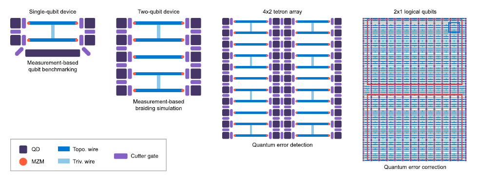
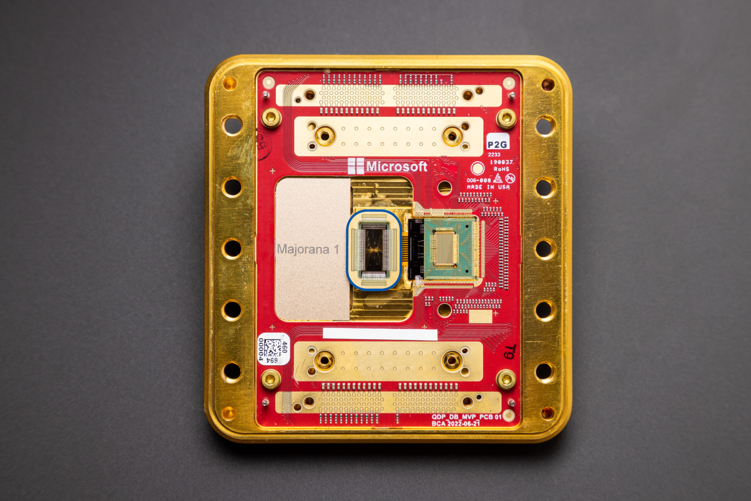
An additional feature of the design is that 99%+ of the electronic circuitry is digital and controlled by a cryoCMOS chip which sits right next to the qubit chip. (You can see the chip in Figure 1. It is the gray looking chip on the green background). The large use of digital signals for control can also make a device simpler and more reliable versus the tuned microwave signals used for control of qubits formed by superconducting transmons.
Each of these qubits fit into a size that is 10 microns x 10 microns and very large devices can be formed by placing these tetrons side by side as shown in Figure 4. Because of the small qubit cell size, one million qubits can be placed in an area in roughly the size of a graham cracker. In Figure 1 above, you can see the large square cutout area that contains the qubit chip in the middle and the words Majorana 1 in the blank area. That architecture is designed such that a chip with one million qubits can fit into that square cutout area.
Measurement Based Quantum Computing with Error Correction
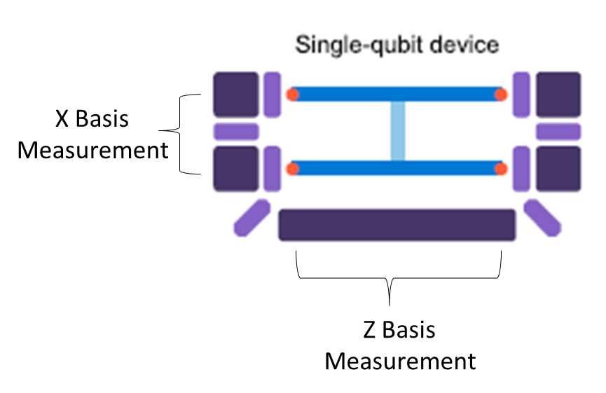
Performing calculations in a topological quantum computer is different than most other quantum computers because it uses Measurement Based Quantum Computing rather than the more common Gate Based Quantum Computing. By performing a series of state measurement one can implement quantum algorithms. Researchers have shown that a measurement-based processor can do everything that a gate based processor can do. As shown in figure 5 below, an X-basis measurement can be performed by making the measurement across two vertical oriented MZMs and a measurement in the Z-basis can be performed by taking the measurement across the two horizontal oriented MZMs. A two qubit measurement for entanglement can be performed by making the measurement between neighboring qubits.
The error rate goal for the physical qubits is an error rate of 10-4. The team has not quite achieved this yet but has plans on how this can be done. The lower the physical error rate one starts with, the easier it is to construct an error correction code that meets the required logical qubit error rate. Microsoft is implementing an error correction code called the Hasting-Haah Floquet code. Error correction codes need to be well-match to the underlying hardware architecture and Microsoft believes that this particular code would be best for their topological processor. With 1 million physical qubits of good quality, the team expects to achieve a thousand logical qubits. Quantum computers of this size will be able to execute commercially useful calculations, particularly for certain computational chemistry applications, that cannot be done classically.
Our Takeaways From this Announcement
- Microsoft has mostly completed the fundamental research stage of this development and is rapidly moving to the engineering implementation phase. There is still a lot of work to do, but most of it involves engineering design and programming work that is not too dissimilar from what is required to create a new classical computer. Some key tasks include additional optimization of the qubit design to further reduce the physical error rate, completing development of the error correction codes to achieve the best logical error rates, more development of all layers of the software stack, and of course, scaling up both the qubit and control logic chips for larger numbers of qubits.
- What is quite striking is to look at all the things they do not have to do to reach one million qubits. A large number of quantum roadmaps we’ve seen require development of a good quantum networking scheme to connect multiple processor modules together with fiber optic cables to create a one million qubit machine. This approach can entail a large number of challenges including transducers, signal loss, transmission fidelity, etc. Since Microsoft plans to fit all one million qubits on one chip they do not have to face these problems for this development. In addition, they may not need to make major changes in the mechanical packaging of the processor from their current Majorana 1 to construct the one million qubit machine. The overall size of the processor complex will be relatively small in comparison to other approaches which helps to reduce certain facility requirements.
- One measure of the goodness of a quantum processor design that everyone ignores is cost per qubit. Although most everyone is highly focused on just developing a quantum computer that is large enough and good enough to provide quantum advantage for a useful application, we believe the quantum industry will eventually become more focused on cost in much the same way the semiconductor and computer industry have done so for the past 70 years. The industry won’t grow very large if the only way to produce a machine that provides a quantum advantage costs a billion dollars. Although the topological qubit chips themselves might be quite expensive, when you are able to put a million qubits on one chip and fit it all into a single dilution refrigerator, the overall cost per qubit will be very, very good.
- As stated in their press release, Microsoft believes they now have a plan to reach the one million qubit benchmark within the next few years. They believe they have identified all the potential challenges they need to surmount and identified approaches for solving them. But what makes this situation a little different than most roadmap announcements that we see is the detailed review by DARPA this program has undergone. In order to be selected for the third stage of the Underexplored Systems for Utility-Scale Quantum Computing (US2QC) program we heard that Microsoft provided hundreds of pages of documentation to DARPA and underwent a review by 40 senior technologists to review their design and plans. The fact that DARPA decided to continue the support for the third phase is a good sign.
Conclusion
So, by no means are we about to say that this development is a slam dunk for the topological approach to win the quantum computing race. There still is a lot of risk involved towards completing the development. There could be new, unanticipated and very difficult problems that could crop up. Or that certain performance goals such as error rates or operation speed may come up short. But the topological computer has now entered the race after standing on the sidelines for many years and presents a viable contender versus all the other solutions people are working on. In any event, we do not expect quantum computing to be a winner take all market and there will be room for multiple solutions in the coming years.
In association with this announcement, Microsoft has published a technical paper in Nature magazine titled Interferometric Single-Shot Parity Measurement in InAs-Al Hybrid Devices and posted a pre-print on arXiv titled Roadmap to fault tolerant quantum computation using topological qubit arrays. Also, they have posted a press release, a blog, videos, and other collateral material that you can find on their website here. Also, the QCR published an earlier article in 2023 about their technology that you might find helpful. It is titled A Deeper Dive Into Microsoft’s Topological Quantum Computer Roadmap and you can access here.
February 19, 2025

I am curious as to the defectivity rates in MBE fabricated structures … Have they been assessed (using defect detection tools standard in CMOS fab, say) and are they already at the level required for the million qubits on one chip? If not, how many orders of magnitude remain to get to 0.01/cm2, say?
As one might expect, Microsoft is keeping certain details of their manufacturing process proprietary for competitive reasons. But here’s what we do know. Microsoft is not currently using a commercial CMOS fab for fabrication such as GlobalFoundries or others. The processing is all performed in their own facilities. The MBE is currently processed at their Quantum Materials Laboratory in Copenhagen, Denmark with additional module construction in Redmond. You can see an announcement from them at https://azure.microsoft.com/en-us/blog/quantum/2018/10/09/accelerating-quantum-materials-research-with-microsofts-new-copenhagen-lab/. They have been working on optimizing this process for many years. For example, we note that a few years ago, they were trying to use InSb for one of the layers in the stack, but now they are using InAs.